Home > SMT Peripheral Equipment
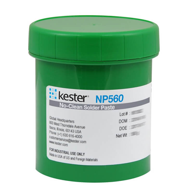
Sn96.5Ag3.0Cu0.5 no-clean Solder Paste NP560
Description:


Sn96 5Ag3Cu0 5 no-clean Solder Paste NP560
Sn96.5Ag3.0Cu0.5 no-clean Solder Paste NP560 is a no-clean, lead-free, halogen-free solder paste. It consistently delivers paste transfer efficiencies of 0.50 to 0.55 AR and is fully capable of printing and reflowing 01005 components, even in air, with minimal graping behavior. In addition to its stable, consistent product performance, NP560 has redefined the voiding standard for PCB assembly and has the potential for low voiding performance.
NP560 Solder Paste
No-Clean, Lead-Free, Low Voiding under QFNs
NP560
Voids:6.6%
Competitor A Voids:36.0%
Competitor B Voids:22.8%
Product Description
NP560 is a no-clean, lead-free, halogen-free solder paste. It consistently delivers paste transfer efficiencies of 0.50 to 0.55 AR and is fully capable of printing and reflowing 01005 components, even in air, with minimal graping behavior. In addition to its stable, consistent product performance, NP560 has redefined the voiding standard for PCB assembly and has the potential for low voiding performance.
Performance Characteristics:
■ Classified as ROL0 per J-STD-004B
■ Halogen-Free
■ Low voiding potential under QFNs
■ Excellent activity and printability
■ Very low graping
■ Reflowable in air and nitrogen
conditions
■ Wide reflow profile window with good solderability on various PCB surface finish
RoHS Compliance
This product meets the requirements of the Restriction of Hazardous Substances (RoHS) Directive. Additional RoHS information is
located at https://www.kester.com/downloads/environmental.
Physical Properties (typical)
Viscosity (typical): 1300 poise
Malcom Viscometer @ 10 rpm, 25°C
Initial Tack: 30gm
Tested per J-STD-005, IPC-TM-650, Method 2.4.44
Cold Slump Test: Pass
Tested per J-STD-005, IPC-TM-650, Method 2.4.35
Hot Slump Test: Pass
Tested per J-STD-005, IPC-TM-650, Method 2.4.35
Solder Ball Test: Pass
Tested per J-STD-005, IPC-TM-650, Method 2.4.43
Wetting: Pass
Tested per J-STD-005, IPC-TM-650, Method 2.4.45
Reliability Properties
Copper Mirror: Low
Tested to J-STD-004, IPC-TM-650, Method 2.3.32
Copper Corrosion: Low
Per IPC-TM-650 Method 2.6.15
Halogen Content: None Detected
Per IPC-TM-650, Method 2.3.81
Silver Chromate: None Detected Tested to J-STD-004, IPC-TM-650, Method 2.3.33
Fluoride Spot Test: None Detected Tested to J-STD-004, IPC-TM-650, Method 2.3.35.1
Surface Insulation Resistance (SIR):
Pass
Per IPC-TM-650 Method 2.6.3.7 [40oC, 90% RH,
12.5V, 7days]
Electrochemical Migration (ECM): Pass Per IPC-TM-650 Method 2.6.14.1 [65oC, 90% RH, 100V, 25days]
Availability
NP560 is available in Sn96.5Ag3Cu0.5 alloy with type 3 and type 4 powder mesh. Type 4 mesh size is recommended for standard and fine pitch applications. NP560 is also compatible with other SnAgCu alloys in similar melting range to the listed alloy. For specific
packaging information, refer to Kester’s Solder Paste Packaging Chart for available sizes. The appropriate combination depends on the process variables and the specific application.
Process Guidelines
Printing Process Parameter
Recommendations
Solder Paste Bead Size
Initial 2cm (0.75in); Add below 1.4cm (0.5in)
Squeegee Angle
60 deg. from horizontal; 45 deg. for pin in paste
Speed
25mm/sec-150mm/sec (1-6in/sec)
Pressure1
0.18-0.27 kg/cm (1-1.5 lb/in)
Separation Speed
2-10mm/sec
Underside Cleaning2
Solvent, vacuum and dry wipe recommended
Stencil Life
8 hours at 65-85°F and 10-70% RH
Reflow Process Parameter
Recommendations
Time from 45°C to peak
3.5-4.5 min
Ramp rate
0.7-2.0°C/sec
Preheat time (130-180°C)
30-90 sec (70 sec target)
Peak temperature
235-255°C for SAC alloys
Cooling Rate
3-6°C/sec
Below information are process guidelines, and it is advisable to note that the optimum setting for a given assembly may vary and this is dependent on the circuit board design, board thickness, components used, and equipment used. A design of experiments is recom- mended to be done to optimize the soldering process.
1 Pressure should be increased with increasing print speed. First set the print speed. Then set the pressure to the minimum required to clean the solder paste off of the stencil.
2 Some cleaning chemistry can interact with the solder paste and can impact print performance.
In addition, incoming solderability inspection of circuit boards and components is recommended as part of process control to maintain consistent soldering performance and electrical reliability.
Note: TAL should be calculated based on the liquidus point of the alloy used: SAC305 221°C. Adding a soak between 180 and 200°C for 20-30 seconds can further reduce voiding and reduce the potential for tombstoning.
The recommended reflow profile for NP560 formula made with SAC alloys is shown
here. This profile is simply a guideline. NP560 has excellent solderability and wetting across a wide range of profiles, with similar performance in air and nitrogen. Your optimal profile may be different from the one shown based on your oven, board and mix of defects. For optimal reflow profile for void reduction or additional profiling advice, contact Kester Technical Support.
Cleaning
NP560 residues are non-conductive, non-corrosive, and do not require removal. If it is desired to remove the residues, commercially available residue cleaner may be used. Contact Kester Technical Support for additional assistance.
Storage, Handling and Shelf Life
Shelf life is 9 months from date of manufacture when stored in refrigeration and can be stored up to 4 weeks at room temperature (up to 27oC/80oF) with minimal impact to overall product performance. Refrigeration (0-10°C/32-50°F) is the recommended storage condi- tion for solder paste to maintain consistent viscosity, reflow characteristics, and overall performance. When refrigerated, NP560 should be stabilized to room temperature prior to use. Kester is continuing with NP560 shelf life study at refrigerated and room temperature storage conditions to validate up to 12 months. Please contact Kester Technical Support if you require additional advice with regards to handling and storage of this material.
Health and Safety
This product, during handling or use, may be hazardous to your health or the environment. Read the Safety Data Sheet and warning label before using this product.
There are various grades of solder paste and the required type can be selected to fit in with the PCB assembly process used. The solder paste is graded according to the size of the small solder balls. As they cannot be exactly graded, the different types have a band of solder ball sizes between which 80% of the minute solder balls fall.
| IPC TYPE DESIGNATION | PARTICLE SIZE (ΜM) * |
|---|---|
| Type 1 | 75 - 150 |
| Type 2 | 45 - 75 |
| Type 3 | 25 - 45 |
| Type 4 | 20 - 38 |
| Type 5 | 10 - 25 |
| Type 6 | 5 - 15 |
| Type 7 | 2 - 11 |
| Type 8 | 2 - 8 |
* 80% minimum between the stated sizes
Solder can also be categorised according to the type of flux used:
In order to ensure that the solder paste is suitable for proving the highest performance for PCB assembly it is necessary to ensure that it maintains the required properties. To achieve this it is imperative that the solder paste is stored correctly. It should always be stored in an airtight container to prevent oxidation. The very large surface area of the minute solder spheres, means that oxidation can present a very great problem.
Additionally, the solder must be stored at low temperatures. Not only does this reduce the rate of any oxidation there may be, but it also reduces the rate at which the flux degrades. While a low temperature is imperative, it should not be stored at a temperature below freezing.
In view of the way in which solder paste can degrade, it also has a defined shelf life and it should not be used after its end date. If old solder paste is used there is a distinct risk of a much higher defect rate, and the cost of any rework incurred would be well beyond the cost of replacing the solder paste.
When solder paste is used in mass PCB assembly as well as prototype PCB assembly there are a number of stages that are undertaken. First solder paste is applied to the printed circuit boards. The solder paste is only applied to the areas where solder is required. This is achieved using a solder paste stencil that only allows the solder paste through in certain areas.
There are many ways of achieving this, but typically a stencil is placed over the board, and the paste is applied though this, ensuring that the required amount is applied - too little and the joints will have sufficient solder - too much and the joints will be too large and there may be the possibility of poor joints and even shorts between adjacent pads, etc.
Once the solder paste has been applied to the printed circuit board, it is then passed into the pick and place machine where the components are added. The solder paste has sufficient tension that it holds the components in place. However care should be taken not to knock the board at this stage otherwise the components may move of fall off. Additionally the board should be soldered within a few hours of being placed, otherwise the solder paste may deteriorate.
Keywords:
SMT Peripheral Equipment, PCB Loader, PCB Unloader, SMT PCB Conveyor, SMT PCB Cleaning Machine, DIP Insert Line, SMT NG/OK Unloader, SMT Shuttle Conveyor.


Contact: Mr Tommy
Phone: +86 13691605420
Tel: +86 -755-85225569
Email: tommy@flason-smt.com
Add: 94#,Guangtian Road,Songgang Street,Bao an District Shenzhen China