Home > SMT Assembly News
SMD or Surface Mount Electronic Components for SMT are no different from through-hole components as far as the electrical function is concerned. Because they are smaller, however, the SMCs (surface mount components) provide better electrical performance.
Not all components are available in surface mount for electronics at this time; hence the full benefits of surface mounting on PCB are not available, ad we are essentially limited to mix-and-match surface mount assemblies. The use of through-hole components such as pin grid array for high end processors and large connectors will keep the industry in mixed assembly mode for the foreseeable future.
Availability of Surface Mount Electronic Components
While only a few types of conventional DIP packages meet all the packaging requirements, the world of surface mount packages is vastly more complex.
The package types and package and lead configurations available are numerous. In addition, the requirements of surface mount components are far more demanding. SMCs must withstand the higher soldering temperatures and must be selected, places, and soldered more carefully to achieve acceptable manufacturing yield.
There are scores of components available for some electrical requirements, causing a serious problem of component proliferation. There are good standards for some components, whereas for others standards are inadequate or nonexistent. Some electronic components are available at a discount, and others carry a premium. While surface mount technology has matured, it is constantly evolving as well with the introduction of new packages. The electronics industry is making progress every day in resolving the economic, technical, and standardization issues with surface mount components. SMDs are available as both active and passive electronic components.
Passive Surface Mount Electronic Components
The world of passive surface mounting is somewhat simpler. Monolithic
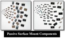
Passive Surface Mount Electronic Components
ceramic capacitors, tantalum capacitors, and thick film resistors form the core group of passive SMD. The shapes are generally rectangular and cylindrical. The mass of the components is about 10 times lower than their through-hole counterparts.
The surface mount resistors and capacitors come in various case sizes to meet the needs of various applications in the electronics industry. While there is a trend toward shrinking case sizes, larger case sizes are also available if capacitance requirements are large. These devices/ components come in both rectangular and tubular (MELF: metal electrode leadless face) shapes.
Surface Mount Discrete Resistors
There are two main types of surface mount resistors: thick film and thin film.
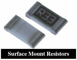
Surface Mount Resistor
Thick film surface mount resistors are constructed by screening resistive film (ruthenium dioxide based paste or similar material) on a flat, high purity alumina substrate surface as opposed to depositing resistive film on a round core as in axial resistors. The resistance value is obtained by varying the composition of resistive paste before screening and laser trimming the film after screening.
In thin film resistors the resistive element on a ceramic substrate with protective coating (glass passivation) on top and solderable terminations (tin-lead) on the sides. The terminations have an adhesion layer (silver deposited as thick film paste) on the ceramic substrate, and nickel barrier underplating followed by either dipped or plated solder coating. The nickel barrier is very important in preserving the solderability of terminations because it prevents leaching (dissolution) of the silver or gold electrode during soldering. Resistors come in 1/16, 1/10, 1/8 and ¼ watt ratings in 1 ohm to 100 megaohm resistance in various sizes and various tolerance. Commonly used sizes are: 0402, 0603, 0805, 1206, and 1210. A surface mount resistor has some form of colored resistive layer with protective coating on one side and generally a white base material on the other side. Thus the outer appearance offers a simple way to distinguish between resistors and capacitors.
Surface Mount Resistor Networks
The surface mount resistor networks or R-packs are commonly used as
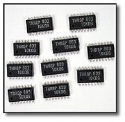
Surface Mount Resistor Networks
replacement for series of discrete resistors. This saves real estate and placement time.
The currently available styles are based on the popular SOIC (Small Outline Integrated Circuits), but the body dimensions vary. They generally come in 16 to 20 pins with ½ to 2 watts power per package.
Ceramic Capacitors for SMT
Surface mount capacitors are ideal for high frequency circuit applications because it does not have any leads and can be placed underneath the package on the opposite side of the PCB. The most widely used packaging for ceramic capacitors is 8 mm tape and reel.
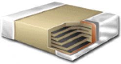
Surface Mount Ceramic Capacitor
Surface mount capacitors are used for both decoupling applications and for frequency control. Multilayer monolithic ceramic capacitors have improved volumetric efficiency. They are available in different dielectric types per EIA RS-198n, namely COG or NPO, X7R, Z5U, and Y5V.
Surface mount capacitors are highly reliable and has been used in high volumes in under-the-hood automotive applications, military equipments and aerospace applications.
Surface Mount Tantalum Capacitors
For Surface Mount capacitors, the dielectric can either be ceramic or tantalum.
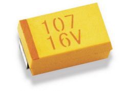
Surface Mount Tantalum Capacitors
Surface mount tantalum capacitors offer very high volumetric efficiency or a high capacitance-voltage product per unit volume and high reliability.
The wrap-under lead capacitors, commonly called plastic molded tantalum capacitors, have leads instead of terminations and a beveled top as a polarity indicator. There are no soldering or placement concerns when using the molded plastic tantalum capacitors. They are available in two case sizes – standard and extended range. The capacitance value for tantalum capacitors vary from 0.1 to 100 µF and from 4 to 50 V dc in different case sizes. They can also be custom made as per the requirement of the application. Tantalum capacitors are available with or without marked capacitance values in bulk, in waffle packs, and on tape and reel.
Tubular Passive Components for SMT
The cylindrical devices known as metal electrode leadless faces (MELFs) are
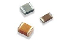
SMD Tubular Passive Components
used for resistors, jumpers, ceramic and tantalum capacitors, and diodes. They are cylindrical and have metal ends caps for soldering.
Since MELFs are cylindrical, the resistors do not have to be placed with resistive elements away from the board surface as is the case with the rectangular resistors. MELFs are less expensive. Like the conventional axial devices, MELFs are color coded for values. MELF diodes are identified as MLL 41 and MLL 34. MELF resistors are identified as 0805, 1206, 1406 and 2309.
SMD Active Components for SMT (Leadless Ceramic Chip Carriers (LCCC), Ceramic Leaded Chip Carriers (CLCC)
Surface mounting offers more types of active and passive packages than
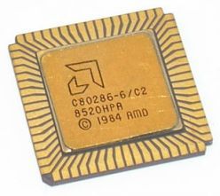
Leadless Ceramic Chip Carrier (LCCC)
through-home mount technology.
Here are all the various categories of active surface mount component packages
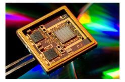
Ceramic Leaded Chip Carrier (CLCC)
family. Others are 40, 25 and 20 mil families.
When leaded ceramic packages are used, their dimensions are generally the same as in plastic leaded chip carriers.
SMD Active Components for SMT (Plastic Packages)
As discussed above, ceramic packages are expensive and are used primarily for military applications. Plastic SMD packages, on the other hand, are most widely used packages for nonmilitary applications, where hermiticity is not required. The ceramic packages have solder joint cracking due to CTE mismatch between the package and the substrate, but the plastic packages are also not trouble free.
Here are all the Active SMD Components (Plastic Packages):
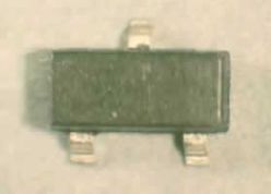
Small Outline Transistors (SOT)
Small Outline Transistors are one of the forerunners of active devices in surface
Small Outline Transistors (SOT)
mounting. They are three- and four-lead devices. The three-lead SOTs are identified as SOT 23 (EIA TO 236) and SOT 89 (EIA TO 243). The four-lead device is known as SOT 143 (EIA TO 253).
These packages are generally used for diodes and transistors. The SOT 23 and SOT 89 packages have become almost universal for surface mounting small transistors. Even as the use of high pin count complex integrated circuits is becoming widespread, the demand for various types of SOTs and SODs continue to grow.
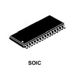
Small Outline Integrated Circuit (SOIC and SOP)
The small outline integrated circuit (SOIC or SO) is basically a shrink package
Small Outline Integrated Circuit (SOIC and SOP)
with leads on 0.050 inch centers. It is used to house larger integrated circuits than is possible in SOT packages. In some cases, SOICs are used to house multiple SOTs.
SOIC contains leads on two sides that are formed outward in what is generally called gull wing lead. SOICs need to be handled carefully to prevent lead damage. SOICs come in mainly two different body widths: 150 mil 300 mils. The body width of packages having fewer than 16 leads is 150 mil; for more than 16 leads, 300 mil widths is used. The 16 lead packages come in both body widths.
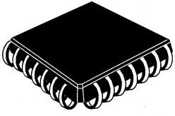
Plastic Leaded Chip Carriers (PLCC)
The plastic leaded chip carrier (PLCC) is a cheaper version of ceramic chipcarrier. The leads in PLCC provide the compliance needed to take up the solder joint stress and thus prevent solder joint cracking. PLCCs with large die-to-package ratios may be susceptible to package cracking due to moisture absorption. They need proper handling.
Plastic Leaded Chip Carriers (PLCC)
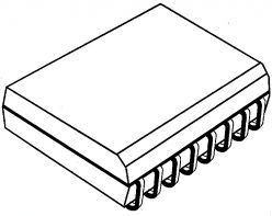
Small Outline J Packages (SOJ)
The SOJ packages have J-bend leads like PLCC, but they have pins on only two sides. This package is a hybrid of SOIC and PLCC and combines the handling benefits of PLCC and space efficiency of SOIC. SOJs are commonly used for high density (1, 4, and 16 MB) DRAMSs.
Small Outline J Packages (SOJ)
Fine Pitch SMD Packages (QFP, SQFP)
SMD packages with very fine pitch and larger number of leads are called fine pitch package. Quad flat pack (QFP) and shrink quad flat pack (SQFP) are examples of fine pitch package. Fine pitch packages have thinner leads and require a thinner land pattern design.
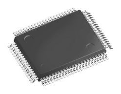
Fine Pitch SMD Packages (QFP, SQFP)
Ball Grid Array (BGA)
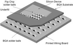
BGA or Ball Grid Array is an array package like PGA (pin grid array) but without the leads.
There are various types of BGAs, but the main categories are ceramic and plastic BGA. The ceramic BGAs are called CBGA (Ceramic Ball Grid Array) and
Ball Grid Array (BGA)
CCGA (Ceramic Column Grid Array), and the plastic BGAs are referred to as PBGA. There is another category of BGA known as tape BGA (TBGA). The ball pitches have been standardized at 1.0, 1.27, and 1.5 mm pitch. (40,50, and 60 mil pitch). The body sizes of BGAs vary from 7 to 50 mm and their pin counts vary from 16 to 2400. Most common BGA pin counts range between 200 and 500 pins.
BGAs are very good for self alignment during reflow even if they are misplaced by 50% (CCGA and TBGA do not self align as well as PBGAs and CBGAs do). This is one reason for the higher yield with BGAs.
Keywords:
SMT Reflow Oven, Lead free Reflow Oven, Reflow Oven Manufacturer, LED reflow oven, PCB Reflow Oven, Nitrogen Reflow Oven, Dual Rail Reflow Oven, China Reflow Oven, wave soldering machine, Dual Rail Wave Soldering Machine, Nitrogen Wave Soldering Machine, Wave Soldering Machine Manufacturer.


Contact: Mr Tommy
Phone: +86 13691605420
Tel: +86 -755-85225569
Email: tommy@flason-smt.com
Add: 94#,Guangtian Road,Songgang Street,Bao an District Shenzhen China