How To Design Cost-Effective PCBs
A design engineer should consider all the things that affect the total cost of manufacturing of PCB. Frequently, new PCB design engineers often do not consider the cost of PCB fabrication. The things that affect the cost per PCB that many young design engineers don't plan for include the cost of tooling, the size of a PCB and the spacing of board components.
To ensure that your production costs are as low as possible, including the costs of tooling, here are some guidelines to follow:
1. Guideline for PCB dimensions
Select the smallest size of the PCB that is practical.
While this seems like a self-evident guideline, not all PCB designers think about it. Remember, the larger the board, the greater the cost. The size of a board has a direct relationship to the final price a customer will pay for it.
2. Guideline for Selecting The Shape of a PCB
Standard rectangular and square PCB shapes always cost less than non-standard shapes. Furthermore, do not incorporate slots or cutouts unless they are completely necessary.
Non-standard shapes often incur upcharges by some PCB fabrication companies. Figure 1 is an example of a custom design that is using a non-standard shaped PCB for mounting within a specialized enclosure. There will always be times when a non-standard PCB shape will be necessary; however, if there is no critical reason why the PCB must be non-standard, always select a standard PCB shape to keep your total costs as low as possible.
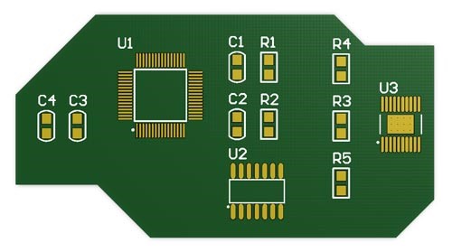
Figure 1: Non-Standard Shaped Printed Circuit Board (PCB)
Figure 2 shows a printed circuit board with a rectangular slot. PCB fabrication companies charge you an extra cost. Figure 2 is a rectangular-slotted PCB. There are upcharges for cutout slots when they are included on PCB by most printed circuit board fabrications companies. In order to keep the total cost of fabricating a PCB low, only use slots when it is critical to the design.
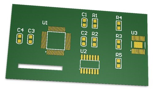
Figure 2: A standard printed circuit board with a slot or cutout made within the PCB.
3. Guidelines for the Size and Separation of Copper PCB Parts
The price of a PCB is increased as the size and separation of the copper parts shrink.
This guideline is the reverse of the first guideline, that is, larger dimensioned copper parts are less expensive. This guideline is obvious because printing parts with very small dimensions require high precision machinery that can handle very small tolerances. In other words, costs are added to a PCB that requires high precision equipment to produce it. This additional cost is escalated when you are producing prototype printed circuit boards that typically have very low production amounts.
The copper parts of concern include SMD or through hole PADS, tracks, vias or other copper layer printed parts. Figure 3 illustrates this issue for pads and tracks. dP represents the separation between the pads while dT represents the separation between the tracks. wT represents the width of the track. Most PCB fabrication companies refer to a standard board with no additional charges when the minimum size of dP, dT and wT varies in the range of 8 to 10 mils (about 0.2mm-0.254mm). To obtain the most cost savings for production purposes, it is wise to limit your design to these ranges. Keep in mind that your can input the physical requirements of these things in most electronic design automation software. Once you've inputted these values into the software, out-of-range errors are prevented from occurring by the design rules checks of the software.
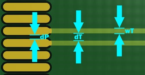
Figure 3: Illustration of Pad and Track Separation Requirements
4. Guidelines for Type of PCB Holes
The cost of producing a PCB increases with small holes and annular rings.
When it is feasible, use larger diameter holes. To manufacture small holes, high precision machines are required; these machines always cost more to use so PCB fabrication houses often add an upcharge for holes less than 0.4 mm. To determine the added cost, you will need to contact the specific fabrication house to learn their policies about additional charges for hole sizes of standard printed circuit boards. To explain this problem better, in figure 4 we have labelled the diameter of the hole with dH.
Minimum angular ring is a vital requirement that refers to through hole pads and vias only, and it is defined as the border of the hole's and the pad's minimum distance. That is, it is the copper rings smallest width that limits the hole. Both Figures four and five demonstrate this concept in detail. Figure four illustrates the concept of the smallest annular ring for circular though hole pads or vias. Figure five illustrates the same concept for pads in an oblong shape.
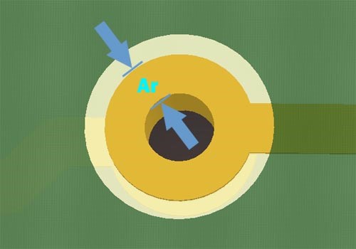
Figure 4: Illustration of annular ring idea for through hole pads or vias
It is critical to be aware that a circular through hole pad or via annular ring width is homogeneous around the hole, while the width of an oblong-shaped through hole is non-homogeneous. Figure five has a red marker to indicate the smallest annular ring.
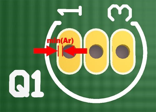
Figure 5: Illustration of a minimum annual ring for an oblong through hole pad
It is important to know that the cost of the PCB will be higher if the minimum annular ring is less than the standard requirements of your PCB fabrication company. Hence, you should ensure that this guideline is inputted into the electronic design automation software you are using before you begin the design of your printed circuit board. Some PCB fabricators will add an upcharge if your minimum annual rings are less than 0.3 mm. Once again, make sure you contact the PCB fabricator to learn their policies regarding this variable, minimum value to ensure it is standard and won't be subject to an additional charge.
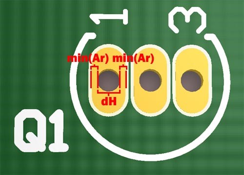
Figure 6: Illustration of an oblong pad's hole diameter and minimum annular ring
Refer to Figure 6 to understand the following equation of the relationship of the size of the pad, size of the hole and the minimum angular ring:
PadMinSize = 2*min(Ar)+dH
The above equation calculates the minimum pad size for a given minimum annular rang and hole diameter. Foe example, if you assume that dH=0.4mm and min(Ar)=0.3mm, then the PadMinSize = 1mm. Hence, a through hole pad less than 1 mm will incur an additional cost.
When using the above equation, take into account that the tolerances of PCB fabrication machines are greater than zero so add some margin to be in the safe size. To consider margin in the above equation, the equation of minimum pad size is modified in the following manner:
PadMinSize = 2*min(Ar)+dH+margin
Generally speaking, margin is normally in the range of 0.05mm - 0.1mm
Concerning vias:
In an earlier article on PCB concepts, it was discussed that vias come in three forms: thru hole, blind and buried. High density and high frequency PCBS that are complex use blind and buried vias. (We will discuss this in more detail in another article). Blind and buried vias are more costly than standard thru hole vias so do not use them unless necessary.
Always contact your PCB fabrication company to verify the minimum requirements for a standard printed circuit board. The values selected for this article are to illustrate the concepts for designing cost-effective PCBs only.
Keywords:
SMT Reflow Oven, Lead free Reflow Oven, Reflow Oven Manufacturer, LED reflow oven, PCB Reflow Oven, Nitrogen Reflow Oven, Dual Rail Reflow Oven, China Reflow Oven, wave soldering machine, Dual Rail Wave Soldering Machine, Nitrogen Wave Soldering Machine, Wave Soldering Machine Manufacturer.
Flason Electronic Co.,ltd provide a full SMT assembly line solutions, including
SMT Reflow Oven,
Wave Soldering Machine,
Pick and Place Machine,
SMT Stencil Printer,
SMT AOI SPI Machine,
SMT Reflow Oven,
SMT Peripheral Equipment,
SMT Assembly line,
SMT Spare Parts
etc any kind SMT machines you may need, please contact us for more information:
wechat whatsapp:+8613691605420, Skype: flasonsmt, Email: sales@flason-smt.com |
 |
 |
 |
FAQ
1) This is the first time I use this kind of machine, is it easy to operate?
There is English manual or guide video that show you how to use machine.
If you still have any question, please contact us by e-mail / skype/ phone /trademanager online service.
2) If machine have any problem after I receive it, how can I do ?
Free parts send to you in machine warranty period.
If the part is less than 0.5KG, we pay the postage.
If it exceeds 0.5KG, you need to pay the postage.
3) MOQ ?
1 set machine, mixed order is also welcomed.
4) How can I buy this machine from you? ( Very easy and flexible !)
A. Consult us about this product on line or by e-mail.
B. Negotiate and confirm the final price , shipping , payment methods and other terms.
C. Send you the proforma invoice and confirm your order.
D. Make the payment according to the method put on proforma invoice.
E. We prepare for your order in terms of the proforma invoice after confirming your full payment.
And 100% quality check before shipping.
F.Send your order by air or by sea.
5)Why choose us ?
A. Gold supplier on Alibaba !
B. Trade assurance to US$54,000 !
C. Best price & Best shipping & Best service ! |
 |