SMT Dictionary – Surface Mount Technology Acronym and Abbreviation
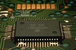
SMT (Surface Mount Technology) is a packaging technology in electronics that mounts electronic components on the surface of a Printed Circuit Board / Printed Wiring Board (PCB / PWB) instead of inserting them through holes of the board. SMT or Surface Mount Technology is relatively new technology in electronics and provides state-of-art, miniature electronics products at reduced weight, volume and cost.
History of SMT is rooted in the technology of Flat Packs (FP) and hybrids of 1950s and 1960s. But for all practical purposes, today’s SMT can be considered

SMT (Surface Mount Technology)
to be a continually evolving technology. Currently the use of Fine Pitch, Ultra Fine Pitch (UFP) and Ball Grid Arrays (BGAs) are becoming even more common.
Even the next level of packaging technologies such as Chip-on-Board (COB), Tape-Automated Bonding (TAB), and Flip Chip Technologies are gainin
Here I explain SMT acronyms and abbreviations.
SMT Dictionary
-
A-Stage: The condition of low molecular weight of a resin polymer during which the resin is readily soluble and fusible.
-
Anisotropic: A material fillet with a low concentration of large conductive particles designed to conduct electricity in the Z axis but not the X or Y axis. Also called Z axis adhesive.
-
Annular Ring: The conductive material around a drilled hole.
-
Aqueous Cleaning: A water-based cleaning methodology which may include the addition of the following chemicals: neutralizers, saponifiers, and surfactants. May also use DI (Deionized) water only.
-
Aspect Ratio: A ratio of the thickness of the board to its preplated diameter. A via hole with aspect ratio greater than 3 may be susceptible to cracking.
-
Azeotrope: A blend of two or more polar and non polar solvents that behaves as a single solvent or remove polar and nonpolar contaminants. It has one boiling point like any other single component solvent, but it boils at a lower temperature than either of its constituents. The constituents of the azeotrope cannot be separated.
-
B. Stage: Sheet material (e.g., glass fabric) impregnated with a resin cured to an intermediate stage.
-
Ball Grid Array (BGA): Integrated circuit package in which the input and output points are solder balls arranged in a grid pattern.
-
Blind Via: A via extended from an inner layer to the surface.
-
Blowhole: A large void in a solder connection created by rapid outgassing during the soldering process.
-
Bridge: Solder that bridges across two conductors that should not be electrically connected, thus causing an electrical short.
-
Buried Via: A via hole connecting internal layers that does not extend to the board surface.
-
Butt Joint: A surface mount device lead that is sheared, so that the end of the leads contacts the board and land pattern.
-
C-Stage Resin: A resin in a final stage of cure.
-
Capillary Action: The combination of force, adhesion, and cohesion which causes liquids such as molten metal to flow between closely spaced solid surfaces against the force of gravity.
-
Castellation: Metallized semicircular radial features on the edges of LCCC’s that interconnect conducting surfaces. Castellations are typically found on four edges of a leadless chip carrier. Each lies within the termination area for direct attachment to the land patterns.
-
CFC: Chlorinated fluorocarbon, cause depletion of ozone layer and scheduled for restricted use by the environmental protection agency. CFC’s are used in air conditioning, foam insulation and solvents, etc.
-
Characteristic Impedance: The voltage-to-current ratio in a propagation wave, i.e., the impedance which is offered to the wave at any point of the line. In printed wiring its value depends on the width of the conductor to ground plane(s) and the dielectric constant to the media between them.
-
Chip Component: Generic term for any two-terminal leadless surface mount passive devices, such as resistors and capacitors.
-
Chip-on-Board Technology: Generic term for any component assembly technology in which an unpackaged silicon die is mounted directly on the printed wiring board. Connections to the board can be made by wire bonding, tape automated bonding (TAB), or flip-chip bonding.
-
CLCC: Ceramic leaded chip carrier.
-
Cold Solder Joint: A solder connection exhibiting poor wetting and a grayish, porous appearance due to insufficient heat or excessive impurities in the solder.
-
Column Grid Array (CGA): Integrated Circuit (IC) package in which the input and output points are high temperature solder cylinders or columns arranged in a grid pattern.
-
Component Side: A term used in through-hole technology to indicate the component side of the PWB.
-
Condensation Inert Heating: A general term referring to condensation heating where the part to be heated is submerged into a hot, relatively oxygen-free vapor. The part, being cooler than the vapor, causes the vapor to condense on the part transferring its latent heat of vaporization to the part. Also known as vapor phase soldering.
-
Constraining Core Substrate: A composite printed wiring board consisting of epoxy-glass layers bound to a low thermal-expansion core material, such as copper-incar-copper, graphite-epoxy, and aramid fiber-epoxy. The core constrains the expansion of the outer layers to match the expansion coefficient of ceramic chip carriers.
-
Contact Angle: The angle of wetting between the solder fillet and the termination or land pattern. A contact angle is measured by constructing a line tangent to the solder fillet that passes through a point of origin located at the place of intersection between the solder fillet and termination or land pattern. Contact angles of less than 90 Degrees Celsius (Positive wetting angles) are acceptable. Contact angles less than 90 Degree Celsius (Negative wetting angles) are unacceptable.
-
Control Chart: A chart that tracts process performance over time. Trends in chart are used to identify process problems that may require corrective action to bring the process under control.
-
Coplanarity: The maximum distance between the lowest and the highest pin when the package rests on a perfectly flat surface. 0.004 inch maximum Coplanarity is acceptable for peripheral packages and 0.008 inch maximum for BGA.
-
Crazing: An internal condition that occurs in the laminated base material in which the glass fibers are separated from the resin at the weave intersections. This condition manifests itself in the form of connected white spots, of “cross,” below the surface of the base material, and is usually related to mechanically induced stress.
-
CTE (Coefficient of Thermal Expansion): The ratio of the change in dimensions to a unit change in temperature. CTE is commonly expressed in ppm/ degree Celsius.
-
Delamination: A separation between plies within the base material, or between the base material and the conductive foil, or both.
-
Dentritic Growth: Metallic filament growth between conductors in the presence of condensed moisture and electrical bias. (Also known as “whiskers.”)
-
Design for Manufacturability: Designing a product to be produced in the most efficient manner possible in terms of time, money, and resources taking into consideration how the product will be produced, utilizing the existing skill base (and avoiding the learning curve) to achieve the highest yields possible.
-
Dewetting: A condition that occurs when molten solder has coated a surface and then receded, leaving irregularly shaped mounds of solder separated by areas covered with a thin solder film. Voids may also be seen in the dewetted areas. Dewetting is difficult to identify since solder can be wetted at some locations and base metal may be exposed at other locations.
-
Dielectric Constant: A property that is a measure of a material’s ability to store electrical energy.
-
DIP (Dual In-Line Package): A package intended for through-hole mounting that has two rows of leads extending at right angles from the base with standard spacing between leads and row.
-
Disturbed Solder Joint: A condition that results from motion between the joined members during solder appearance, although they may also appear lustrous.
-
Drawbridging: A solder open condition during reflow in which chip resistors and capacitor resemble a draw bridge.
-
Dual-Wave Soldering: A wave soldering process that uses a turbulent wave with a subsequent laminar wave. The turbulent wave ensures complete solder coverage in tight areas and the laminar wave removes bridges and icicles. Designed for soldering surface mount devices glued to the button of the board.
-
Electroless Copper: Copper plating deposited from a plating solution as a result of a chemical reaction and without the application of an electrical current.
-
Electrolytic Copper: Copper plating deposited from a plating solution by the application of an electrical current.
-
Etchback: The controlled removal of all components of base material by a chemical process on the side walls of holes in order to expose additional internal conductor areas.
-
Eutectic: The alloy of two or more metals that has a lower melting point than either of its constituents. Eutectic alloys, when heated, transform directly from a solid to a liquid and do not show pasty regions.
-
Fiducial: A geometric shape incorporated in the artwork of a printed wiring board, and used by a vision system to identify the exact artwork location and orientation. Generally three fiducial marks are used per board. Fiducial marks are necessary for the accurate placement of fine pitch packages. Both global and local fiducials can be used. Global fiducials (generally three) locate the overall circuitry pattern to the PCB, whereas local fiducials (one or two) are used at component locations, typically fine pitch patterns, to increase the placement accuracy. Also known as alignment target.
-
Fillet: (1) A radius or curvature imparted to inside meeting surfaces. (2) The concave junction formed by the solder between the footprint pad and the SMC lead or pad.
-
Fine Pitch: A center to center lead distance of surface mount packages of 0.025 inch or less.
-
Flatpack: An integrated circuit package with gull wing or flat leads on two or four sides, with standard spacing between leads. Commonly the leads pitches are at 50 mil centers, but lower pitches may also be used. The packages with lower pitches are generally referred to as fine pitch packages.
-
Flip-Chip Technology: A chip-on-board technology is which the silicon die is inverted and mounted directly to the printed wiring board. Solder is deposited on the bonding pads in vacuum. When inverted, they make contact with the corresponding board lands and the die rests directly above the board surface. It provides the ultimate is densification also known as C4 (controlled collapse chip connection).
-
Footprint: A nonpreferred term for Land Pattern.
-
Functional Test: A electrical test of an entire assembly that stimulates the intended function of the product.
-
Glass Transition Temperature: The temperature at which a polymer changes from a hard and relatively brittle condition to a viscous or rubbery condition. This transition generally occurs over a relatively narrow temperature range. It is not a phase transition. In this temperature region, many physical properties undergo significant and rapid changes. Some of those properties are hardness, brittleness, thermal expansion, and specific heat.
-
Gull Wing Lead: A lead configuration typically used on small outline packages where leads bend and out. An end view of the package resembles a gull in flight.
-
Icicles (Solder): A sharp point of solder that protrudes out of a solder joint, but does not make contact with another conductor. Icicles are not acceptable.
-
In-Circuit Test: A electrical test of an assembly in which each component is tested individually, even though many electronic components are soldered to the board.
-
Ionograph: An instrument designed to measure board cleanliness (the amount of ions present on a surface). It extracts ionizable materials from the surface of the part to be measured and records the rate of extraction and the quantity.
-
JEDEC: Joint Electronic Devices Engineering Council.
-
J-Lead: A lead configuration typically used on plastic chip carrier packages which have leads that are bent underneath the package body. A side view of the formed lead resembles the shape of the letter “J”.
-
Known Good Die: Semiconductor die that has been tested and is known to function to specification.
-
Laminar Wave: A smoothly flowing solder wave with no turbulence.
-
Land: A portion of a conductive pattern usually, but not exclusively, used for the connection, or attachment, or both of components. (Also called a “pad”).
-
Land Pattern: Component mounting sites located on the substrate that is intended for the interconnection of a compatible Surface Mount Component. Land patterns are also referred to as “lands” or “pads”.
-
LCC: A nonpreferred term for “leadless ceramic chip carrier”.
-
LCCC (Leadless Ceramic Chip Carrier): A ceramic, hermetically-sealed, integrated circuit (IC) package commonly used for military applications. The package has Metallized castellations on four sides for interconnecting to the substrate. (Also known as LCC).
-
Leaching: The dissolution of a metal coating, such as silver and gold, into liquid solder. Nickel barrier interplating is used to prevent leaching. Also known as scavenging.
-
Lead Configuration: The solid formed conductors that extend from a component and serve as a, mechanical and electrical connection that is readily formed to a desired configuration. The gull wing and J-lead are the most common surface mount lead configurations. Less common are butt leads formed by cutting standard DIP package leads at the knee.
-
Lead Pitch: The distance between successive centers of the leads of a component package.
-
Legend: Letters, numbers, symbols, and/or patterns on the PCB that are used to identify component locations and orientation for aid in assembly and rework / repair operations.
-
Manhattan Effect: A solder open condition during reflow in which chip resistors and capacitor resemble a draw bridge.
-
Mass Lamination: The simultaneous lamination of a number of pre-etched, multiple image, C-stage panels or sheets, sandwiched between layers of prepeg (B-stage) and copper foil.
-
Mealing: A condition at the interface of the conformal coating and base material, in the form of discrete spots or patches, which reveals a separation of the conformal coating from the surface of the printed board (PCB), or from the surfaces of attached components, or from both.
-
Measling: An internal condition that occurs in laminated base material in which the glass fibers are separated from the resin at the weave intersection. This condition manifests itself in the form of discrete white spots or “crosses” below the surface of the base material, and is usually related to the thermally induced stress.
-
MELF: A metal electrode leadless face surface mount device that is round, cylindrical passive component with a metallic cap termination located at each end.
-
Metallization: A metallic deposited on substrates and component terminations by itself, or over a base metal, to enable electrical and mechanical interconnections.
-
Multichip Module (MCM): A circuit comprised of two or more silicon devices bonded directly to a substrate by wire bond, TAB, or flip chip.
-
Multilayer Board: A Printed Wiring Board (PWB/PCB) that uses more than two layers for conductor routing. Internal layers are connected to the outer layers by way of plated via holes.
-
Neutralizer: An alkaline chemical added to water to improve its ability to dissolve organic acid flux residue.
-
No-Clean Soldering: A soldering process that uses a specially formulated solder paste that does not require the residues to be cleaned after solder processing.
-
Node: An electrical junction connection two or more component terminations.
-
Nonwetting: A condition whereby a surface has contacted molten solder, but has had part or none of the solder adhere to it. Nonwetting is recognized by the fact that the bare base metal is visible. It is usually caused by the presence of contamination on the surface to be soldered.
-
Omegameter: An instrument used to measure board cleanliness (ionic residues on the surface of PCB assemblies). The measurement is taken by immersing the assembly into a predetermined volume of a water-alcohol mixture with a known high resistivity. The instrument records and measures the drop of resistivity caused by ionic residue over a specified period of time.
-
Ounces of Copper: This refers to the thickness of copper foil on the surface of the laminate: ½ ounce copper, 1 ounce copper, and 2 ounce copper are common thickness. One ounce copper foil contains 1 ounce of copper per square foot of foil. The foil on the surface of the laminate may be designated for the copper thickness on both sides by: 1/1 = 1 ounce, two sides; 2/2 = 2 ounces, two sides; and 2/1 = 21 ounce on one side and 1 ounce on the other side. ½ ounce = 0.72 mil = 0.00072 inch; 1 ounce = 1.44 mils = 0.00144 inch; 2 ounces = 2.88 mils = 0.00288 inch.
-
Outgassing: De-aeration or other gaseous emission from a PCB or solder joint.
-
PAD: A portion of a conductive pattern usually, but not exclusively, used for the connection, attachment, or both of components. Also called a “Land”
-
Pin Grid Array (PGA): Integrated circuit package in which the input and output points are through-hole pins arranged in a grid pattern.
-
P/I Structure: Packaging and interconnecting structure
-
PLCC (Plastic Leaded Chip Carrier): A components package that has J-leads on four sides with standard spacing between leads.
-
Prepreg: Sheet material (e.g., glass fabric) impregnated with a resin cured to an intermediate stage (B-stage resin).
-
Printed Circuit Board (PCB) / Printed Wiring Board (PWB): The general term for completely processed printed circuit configuration. It includes rigid or flexible, single, double, or multilayer boards. A substrate of epoxy glass, clad metal, or other material upon which a pattern of conductive traces is formed to interconnect electronic components. Printed Wiring Assembly (PWA): A printed wiring board on which separately manufactured components are parts have been added. The generic term for a printed wiring board after all electronic components have been completely attached / soldered. Also called “printed circuit assembly”.
-
Profile: A graph of time versus temperature.
-
PTH (Plated Through Hole): A plated via used as an interconnection between top and bottom sides or inner layers of a PWB/PCB. Intended for mounting component leads into through-hole technology.
-
Quadpack: Generic term for SMT packages with leads on all four sides. Most commonly used to describe packages with gull wing leads. Also known as flat pack, but flat packs may have gull wing leads on either two or four sides.
-
Reference Designator: A combination of letter and numbers that identify the class of the component on an assembly drawing.
-
Reflow Soldering: A process of joining metallic surfaces (without the melting of base metals) through the mass heating of preplaced solder paste to solder fillets in the Metallized area.
-
Resin Recession: The presence of voids between the barrel of the plated through hole and the wall of the holes, seen in cross-sections of plated through holes in boards that have been exposed to high temperatures.
-
Resin Smear: A condition usually caused by drilling in which the resin is transferred from the base material to the wall of a drilled hole covering the exposed edge of the conductive pattern. Resist: Coating material used to mask or protect selected areas of a pattern from the action of an etchant, solder, or plating.
-
Saponifier: An alkaline chemical, when added to water, makes it soapy and improves its ability to dissolve rosin flux residue.
-
Secondary Side: the side of the assembly that is commonly referred to as the solder side in through hole technology. In SMT, the secondary side may be either reflow soldered (active components) or wave soldered (passive components).
-
Self-Alignment: Due to the surface tension of molten solder, the tendency of slightly misaligned components (during placement) to self align with respect to their land pattern during reflow soldering. Minor self-alignment is possible, but one should not count on it.
-
Semi-Aqueous Cleaning: This cleaning technique involves a solvent cleaning step, hot water rinses, and a drying cycle.
-
Shadowing (Solder): A condition in which solder fails to wet the surface mount device leads during wave soldering process. Generally the trailing terminations of a component are affected, because the component body blocks the proper flow of solder. Requires proper component orientation during wave soldering to correct the problem.
-
Shadowing (Infrared Reflow): A condition in which component bodies block radiated infrared energy from striking certain areas of the board directly. Shadowing areas receive less energy than their surroundings and may not reach a temperature sufficient to completely melt the solder paste.
-
Single-Layer Board: A PWB that contains Metallized conductors on only one side of the board. Through-holes are unplated.
-
Single-Wave Soldering: A wave soldering process that uses only a single, laminar wave to form the solder joints. Generally not used for wave soldering.
-
SMC: A surface mount component
-
SMD: A surface mount device. Registered service mark of North American Philips Corporation to denote resistor, capacitor, SOIC and SOT.
-
SMOBC (Solder Mask Over Bare Copper): The technology of using solder mask to protect the external bare copper circuitry from oxidation, and for coating the exposed copper circuitry with tin-lead solder.
-
SMT (Surface MountTechnology): A method of assembling printed wiring boards or hybrid circuitry, where components are mounted onto the surface rather than inserted into through-holes.
-
SOIC (Small Outline Integrated Circuit): An integrated surface mount package with two parallel rows of gull-wing leads, with standard spacing between leads and rows.
-
SOJ (Small Outline J-Leaded): An integrated circuit surface mount package with two parallel rows of J-Leads, with standard spacing between leads and rows. Generally used for memory devices.
-
Solder Balls: Small spheres of solder adhered to laminate, mask, or conductors. Solder Balls are most often associated with the usage of solder paste containing oxides. Baking of paste may minimize formation of solder balls, but overbaking may cause excessive balling.
-
Solder Bridging: The undesirable formation of a conductive path by solder between conductors.
-
Solder Fillet: A general term used to describe the configuration of a solder joint that was formed with a component lead or termination and a PWB land pattern.
-
Solder Flux: Solder flux or simply flux is a kind of chemical used by electronic companies in electronics industry to clean surfaces of PCB before soldering electronic components onto the board. The main function of using flux in any PCB assembly or rework is to clean and remove any oxide from the board.
-
Solder Paste / Solder Cream: A homogeneous combination of minute spherical solder particles, flux, solvent, and a gelling or suspension agent used in surface mount reflow soldering. Solder paste can be deposited on a substrate via solder dispensing and screen or stencil print.
-
Solder Side: A term used in through-hole technology to indicate the soldered side of PWB.
-
Solder Wicking: The capillary action of molten solder to a pad or component lead. In the case of leaded packages, excessive wicking can lead to an insufficient amount of solder at the lead/pad interface. It is caused by rapid heating during reflow or excessive lean Coplanarity, and is more common in the vapor phase than in IR soldering.
-
Solvent: Any solution capable of dissolving a solute. In the electronics industry, aqueous, semi-aqueous and non-ozone-depleting solvents are used.
-
Solvent Cleaning: The removal of organic and inorganic soils using a blend of polar and nonpolar organic solvents.
-
SOT (Small Outline Transistor): A discrete semiconductor surface mount package that has two gull wing leads on one side of the package and one on the other side.
-
Squeegee: A rubber or metal blade used in screen and stencil printing to wipe across the screen/stencil to force the solder paste through the screen mesh or stencil apertures onto the land pattern of the PCB. Stencil: A thick sheet of Metallic Material with a circuit pattern cut into it.
-
Surface Insulation Resistance (SIR): A measure in ohms of the insulating material’s electrical resistance between conductors.
-
Surfactant: Contracting of “Surface active agent.” A chemical added to water in order to lower surface tension and allow penetration of water under tighter spaces.
-
TAB (Tape Automated Bonding): The process of mounting the integrated circuit die directly on the surface of the substrate, and interconnecting the two together using a fine lead frame.
-
Tape Carrier Package (TCP): Same as TAB
-
Tenting: A printed board fabrication method of covering over plated via holes and the surrounding conductive pattern with a resist, usually dry film.
-
Termination: The metallization surfaces, or in some cases, metal end clips on the end of passive chip components.
-
Thixotropic: The characteristic of a liquid or gel that is viscous when static, yet fluid when physically “worked.”
-
Tombstoning: Same as Drawbridging.
-
Type I SMT Assembly: An exclusive SMT PCB assembly with components mounted on one or both sides of the substrate.
-
Type II SMT Assembly: A mixed technology PCB assembly with SMT components mounted on one or both sides of the substrate and through-hole components mounted to the primary or component side.
-
Type III SMT Assembly: A mixed technology PCB assembly with passive SMT components and occasionally SOICs (small outline integrated circuits) mounted on the secondary side of the substrate and through-hole components mounted to the primary or component side. Typically this type of assembly is wave soldered in a single pass.
-
Ultra Fine Pitch: A center lead distance of surface mount packages of 0.4mm or less.
-
Vapor Phase Soldering: Same as Condensation Inert Heating.
-
Via Hole: A plated through hole connecting two or more conductor layers of a multilayer PCB. There is no intention to insert a component lead inside a via hole.
-
Void: The absence of material in a localized area.
-
Wave Soldering: A process of joining metallic surfaces (without the melting of the base metals) through the introduction of molten solder to metallized areas. Surface mount devices are attached using adhesive and are mounted on the secondary side of the PWB.
-
Weave Exposure: A surface condition of base material in which the unbroken fibers of woven glass cloth are not completely covered by resin.
-
Wetting: A physical phenomenon of liquids, usually in contact with solids, wherein the surface tension of the liquid has been reduced so that the liquid flows and makes intimate contact in a very thin layer over the entire substrate surface. Regarding wetting of a metal surface by a solder flux reduces the surface tension of the metal surface and the solder, resulting in the droplets of solder collapsing into a very thin film, spreading, and making intimate contact over the entire surface.
-
Wicking: Absorption of liquids by capillary action along the fibers of the base metal.
Keywords:
SMT Reflow Oven, Lead free Reflow Oven, Reflow Oven Manufacturer, LED reflow oven, PCB Reflow Oven, Nitrogen Reflow Oven, Dual Rail Reflow Oven, China Reflow Oven, wave soldering machine, Dual Rail Wave Soldering Machine, Nitrogen Wave Soldering Machine, Wave Soldering Machine Manufacturer.
Flason Electronic Co.,ltd provide a full SMT assembly line solutions, including
SMT Reflow Oven,
Wave Soldering Machine,
Pick and Place Machine,
SMT Stencil Printer,
SMT AOI SPI Machine,
SMT Reflow Oven,
SMT Peripheral Equipment,
SMT Assembly line,
SMT Spare Parts
etc any kind SMT machines you may need, please contact us for more information:
wechat whatsapp:+8613691605420, Skype: flasonsmt, Email: sales@flason-smt.com |
 |
 |
 |
FAQ
1) This is the first time I use this kind of machine, is it easy to operate?
There is English manual or guide video that show you how to use machine.
If you still have any question, please contact us by e-mail / skype/ phone /trademanager online service.
2) If machine have any problem after I receive it, how can I do ?
Free parts send to you in machine warranty period.
If the part is less than 0.5KG, we pay the postage.
If it exceeds 0.5KG, you need to pay the postage.
3) MOQ ?
1 set machine, mixed order is also welcomed.
4) How can I buy this machine from you? ( Very easy and flexible !)
A. Consult us about this product on line or by e-mail.
B. Negotiate and confirm the final price , shipping , payment methods and other terms.
C. Send you the proforma invoice and confirm your order.
D. Make the payment according to the method put on proforma invoice.
E. We prepare for your order in terms of the proforma invoice after confirming your full payment.
And 100% quality check before shipping.
F.Send your order by air or by sea.
5)Why choose us ?
A. Gold supplier on Alibaba !
B. Trade assurance to US$54,000 !
C. Best price & Best shipping & Best service ! |
 |
